|
|
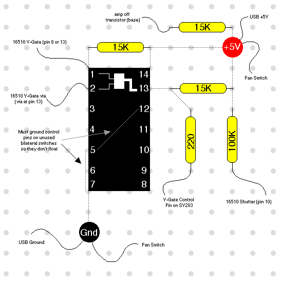 |
Circuit diagram
Click to enlarge.
|
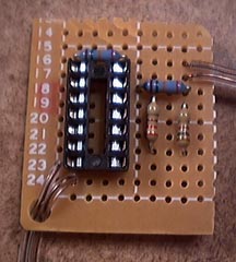 |
The top of my circuit board. One of the resistors isn't in place yet, and of course the 4066 chip hasn't been inserted into the socket yet.
|
 |
A remarkably uninformative image of the bottom of the circuit board.
|
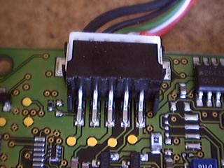 |
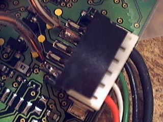
Here's where the USB cable attaches to the main board.
|
 |
And here it is with the power wires soldered to it. They provide power to the circuit board. The +5V is provided by the red lead on one end. The ground is the fourth lead over from the +5V wire. I doused these connections in glue after soldering them to protect them from breaking off.
|
