Logitech Quickcam Pro 3000 Long Exposure Modification
Modifying the Webcam Circuitry
In order to work on the webcam, it helps to fix it face down to a heavy flat surface. I did this by removing the entire lens assembly (including the lens holder that contains the ir filter, which is held on by two screws that go through the circuitboard), taping a piece of lens paper over the ccd for protection, and then taping the circuitboard face down to a heavy flat surface (a book will do nicely).
There are several steps separated into two major stages: severing connections that already exist, and making connections that don't yet exist. Two connections must be severed, four must be made (to either side of the severed connections so that you will resultantly have explicit control -- in the form of on/off switches -- over the electrical pathways that previously flowed unimpeeded through those two connections).
|
|
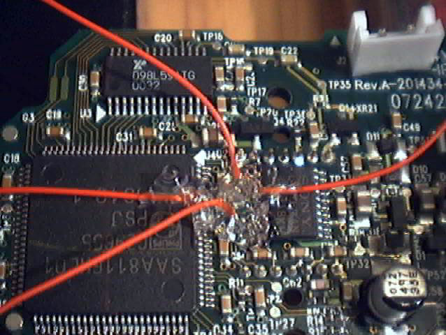
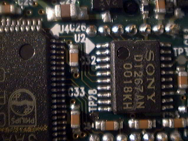 |
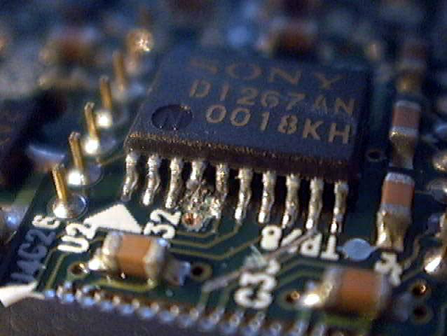
The area you will be working in. The SAA chip is on the left, the CXD chip is on the right.
Click to enlarge.
|
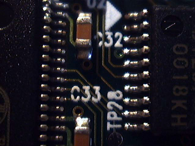 |
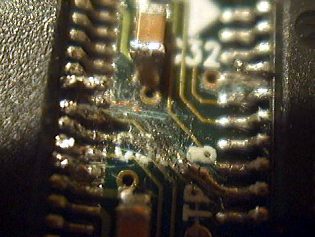
A closeup of the working area.
Click to enlarge.
|
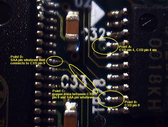 |
A technical overlay of the working area:
Point A: pin 4 must be lifted, then wires must be soldered to the lift pin and to pin 4's pad or the via connected to the pad. This is the "shutter" control and the shutter switch will be connected to this point.
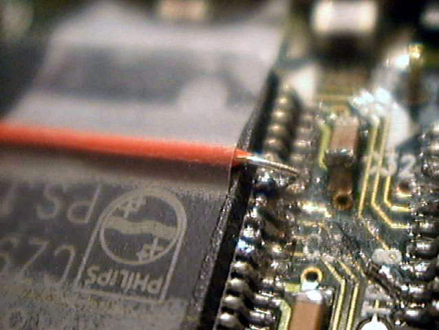
Point B: a wire must be soldered to pin 9 (or alternatively you could solder to an exposed piece of the trace next to the pin, or alternatively, you could lift the pin and then solder to it, whichever solution you find easiest).
Points C and D: read the detailed description below for more on these points.
Points B, C, and D are the "v-gate exposure" control and the v-gate switch will be connected to these points.
Click to enlarge.
|
Point A is simple to understand, if difficult to implement. Pin 4 must be lifted to break its connection to its pad, and by consequence, to break its connection to the via connected to the pad. Then, pieces of wire must be soldered to the lifted pin and to the pad or the via (doesn't matter which).
Point B is simple but offers options depending on how you do points C and D. Basically, two high-level things must be done and there are several ways this might be accomplished. There is an electrical connection from the SAA to the CXD running through the trace marked as point C. This connection must be severed by some means and then wires must be connected to either side of the connection. This can be done in several ways. If you expose the copper trace by scraping through the circuitboard and then cut the copper trace, you don't need to lift the pins on the SAA or the CXD. You can then solder either to the pins, or to the exposed copper trace. Alternatively, you can lift either pin (or both pins) and subsequently solder wires to the lifted pins or to the copper trace if one of the pins is left unlifted (so the pin is still connected to the trace). It's completely up to you. Just pick a solution that you are comfortable with.
You will see in the next few pictures that I attempted Martin's method, which was to cut the copper trace and the solder to it. This was a complete disaster. Soldering to the copper trace is nearly impossible. I ultimately gave up on that, after virtually destroying the circuitboard and putting solder bridges all over the place that I subsequently had to fix. My eventual solution was to lift the pin on the SAA and then solder the wire directly to that lifted pin. Despite the fact that the pins on the SAA are even tinier than the pins on the CXD, this was still easier than trying to solder to the damn trace.
|
|
 |
Using an x-acto blade with a sharp angled point scrape out the via at Point A and expose the trace at Point C. If you look at this picture carefully (and enlarged) you will see that I have indeed cut completely through the trace, thus severing its connection). Even though the traces are visually marked with gold lines, these are not open electrical wires. The gold lines are a coating on the surface of the circuitboard. You must scrape through them and expose the bare copper underneath to make an electrical connection (you must do this anyway to cut through the trace and sever the connection). Test that the connection has been severed with the continuity function on a multimeter.
Click to enlarge.
|
 |
Lift the pin at Point A. Some people do this with a soldering iron, but it's a million times easier to slowly wedge the x-acto blade under the pin from both sides until the pin loosens and eventually becomes free. Then you can lift it up. Be sure to clean out the area under the pin so there is no residual connection to the pad. Test that the connection is broken with the contuinity function on a multimeter.
Click to enlarge.
|
 |
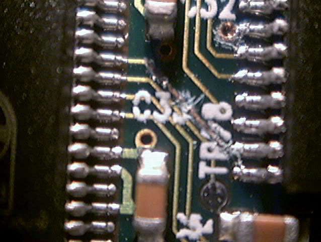
A lot has happened at this point. Notice that I have virtually destroyed the copper trace at point C trying to solder a wire to it. The trace is almost completely empty now, leaving me nothing left to solder to. So, I lifted the pin on the left (on the SAA) with the intention of soldering to it. I lifted the pin simply because it is much easier to solder to the pin once it is lifted. There isn't much risk of creating a solder bridge to the neighboring pins that way. Also notice that I have a nice big glop of solder attached to pin 9 at Point B. I will use this to solder a wire to pin 9.
Click to enlarge.
|
 |
Here is how I solder a wire to the lifted pin on the SAA (same thing goes for the lifted pin at Point A on the CXD. Tape the wire down so it won't move around. Bend it slightly so it rests next to the lifted pin. Then touch a small ball of solder to the pair and the connection will quickly and effortlessly be made.
Click to enlarge.
|
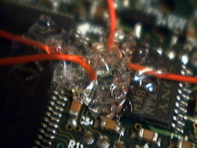 |
I have gone ahead and made the remaining three connections and covered the entire area with hot glue so the solder joints won't come free. Incidently, it was very difficult to solder a wire to the via at Point A, so I eventually gave up, inserted the wire deep into the via, and simply glued over it, holding the wire tightly inside the via. This worked just fine.
Click to enlarge.
|
 |
Another picture of the completed mod showing how is situates on the rest of the circuitboard. The hot glue released from the backs of the two ICs after a day or two, so I was forced to fill in the gap between the hunks of dried hot glue and the ICs with a tiny drop of superglue (which runs everywhere making a big mess, perhaps the superglue gel would have worked better). The superglue held the pins and the hot glue down to the ICs perfectly and doesn't appear to have damaged the circuitboard, but I have my concerns about this approach. Superglue is pretty acidic stuff (have you ever caught a whiff of it?). I wonder if it could eat through the delicate electronics if it got into the wrong crevice.
Click to enlarge.
|
